

Xilinx SoC overview and history
In the early 2000s, Xilinx introduced the concept of building embedded processors into its available FPGAs at the time, namely the Spartan-2, Virtex-II, and Virtex-II Pro families. Xilinx brought two flavors of these early SoCs to the market: a soft version and an initial hard macro-based option in the Virtex-II Pro FPGAs.
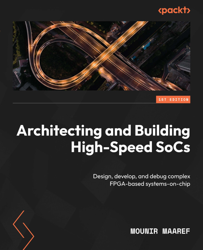
The soft flavor uses MicroBlaze, a Xilinx RISC 32-bit based soft processor coupled initially with an IBM-based bus infrastructure called CoreConnect and a rich set of peripherals, such as a Gigabits Ethernet MACs, PCIe, and DDR DRAM, just to name a few. A typical MicroBlaze soft processor-based SoC looks as follows:
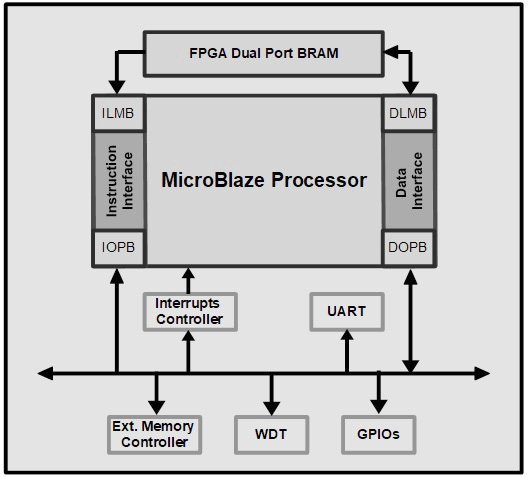
Figure 1.2 – Legacy FPGA MicroBlaze embedded system
The hard macro version uses a 32-bit IBM PowerPC 405 processor. It includes the CPU core, a memory management unit (MMU), 16 KB L1 data and 16 KB L1 instruction caches, timer resources, the necessary debug and trace interfaces, the CPU CoreConnect-based interfaces, and a fast memory interface known as on-chip memory (OCM). The OCM connects to a mapped region of internal SRAM that’s been built using the FPGA block RAMs for fast code and data access. The following diagram shows a PowerPC 405 embedded system in a Virtex-II Pro FPGA device:
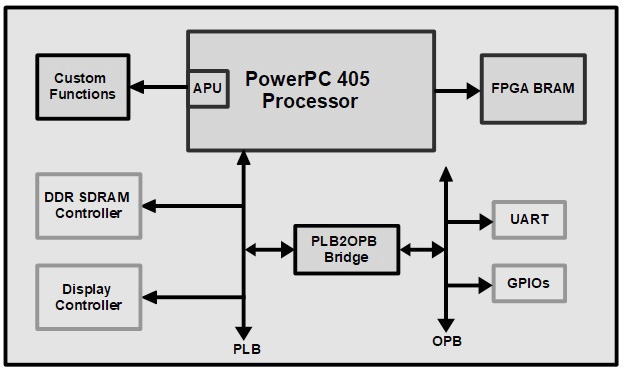
Figure 1.3 – Virtex-II Pro PowerPC405 embedded system
Embedded processing within FPGAs has received a wide adoption from different vertical spaces and opened the path to many single-chip applications that previously required the use of an external CPU, alongside the FPGA device, as the main board processor.
The Virtex-4 FX was the next generation to include the IBM PowerPC 405 and improved its core speed.
The Virtex-5 FXT followed and integrated the IBM PowerPC 440x5 CPU, a dual-issue superscalar 32-bit embedded processor with an MMU, a 32 KB instruction cache, a 32 KB data cache, and a Crossbar interconnect. To interface with the rest of the FPGA logic, it has a processor local bus (PLB) interface, an auxiliary processor unit (APU) for connecting FPU, and a custom coprocessor built into the FPAG logic. It also has a high-speed memory controller interface. With the Ethernet Tri-Speed 10/100/1000 MACs integrated as hardware functional blocks in the FPGA, we started seeing the main ingredients necessary for making an SoC in FPGAs, with most of the logic-consuming hardware functions now bundled together around the CPU block or delivered as a hardware functional block that just needs interfacing and connecting to the CPU. This was a step close to a full SoC in FPGAs. The following diagram shows a PowerPC 440 embedded system in a Virtex-5 FXT FPGA device:
Figure 1.4 – Virtex-5 FXT PowerPC440 embedded system
The Virtex-5 FXT was the last Xilinx FPGA to include an IBM-based CPU; the future was switching to ARM and providing a full SoC in FPGAs with the possibility to interface to the FPGA logic through adequate ports. This offered the industry a new kind of SoC that, within the same device, combined the power of an ASIC and the programmability of the Xilinx-rich FPGAs. This brings us to this book’s main topic, where we will delve into and try to deal with all Xilinx’s related design development and technological aspects while taking an easy-to-follow and progressive approach.
The following diagram illustrates the approach taken by Xilinx to couple an ARM-based CPU SoC with the Xilinx FPGA logic in the same chip:
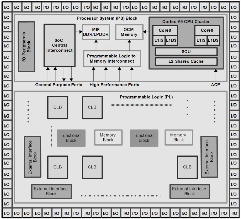
Figure 1.5 – Zynq-7000 SoC FPGA conceptual diagram
A short survey of the Xilinx SoC FPGAs based on an ARM CPU
The first device family that Xilinx brought to the market for integrating an ARM Cortex-A9 CPU was the Zynq-7000 FPGA. The Cortex-A9 is a 32-bit processor that implements the ARMv7-A architecture and can run many instruction formats. These are available in two configurations: a single Cortex-A9 core in the Zynq-7000S devices and a dual Cortex-A9 cluster in the Zynq-7000 devices.
The next generation that followed was the Zynq UltraScale+ MPSoC devices, which provide a 64-bit ARM CPU cluster for integrating an ARM Cortex-A53, coupled with a 32-bit ARM Cortex-R5 in the same SoC. The Cortex-A53 CPU implements the ARMv8-A architecture, while the Cortex-R5 implements the ARMv7 architecture and, specifically, the R profile. The Zynq UltraScale+ MPSoC comes in different configurations. There is the CG series with a dual-core Cortex-A53 cluster, the EG series with a quad-core Cortex-A53 cluster and an ARM MALI GPU, and the EV series, which comes with additional video codecs to what is available in the EG series.
A few years ago, Xilinx also launched a version of the MPSoC with key components to help build advanced radio connectivity SoCs: the Zynq UltraScale+ RFSoC.