


Xilinx Zynq Ultrascale+ MPSoC family overview
The Zynq UltraScale+ MPSoC is the second generation of the Xilinx SoC FPGAs based on the ARM CPU architecture. Like its predecessor, the Zynq-7000 SoC, it is based on the approach of combining the FPGA logic HW configurability and the SW programmability of its ARM CPUs but with improvements in both the FPGA logic and the ARM processor CPUs, as well as its PS features. The UltraScale+ MPSoC offers a heterogeneous topology that couples a powerful 64-bit application processor (implementing the ARMv8-A architecture) and a 32-bit real-time R-profile processor.
The PS includes many types of processing elements: an APU, such as the dual-core or quad-core Cortex-A53 cluster, the dual-core Cortex-R5F real-time processing unit (RPU), the Mali GPU, a PMU, and a video codec unit (VCU) in the EG series. The PS has an efficient power management scheme due to its granular power domains control and gated power islands. The Zynq UltraScale+ MPSoC has a configurable system interconnect and offers the user overall flexibility to meet many application requirements. The following diagram provides an architectural view of the Zynq UltraScale+ SoC:
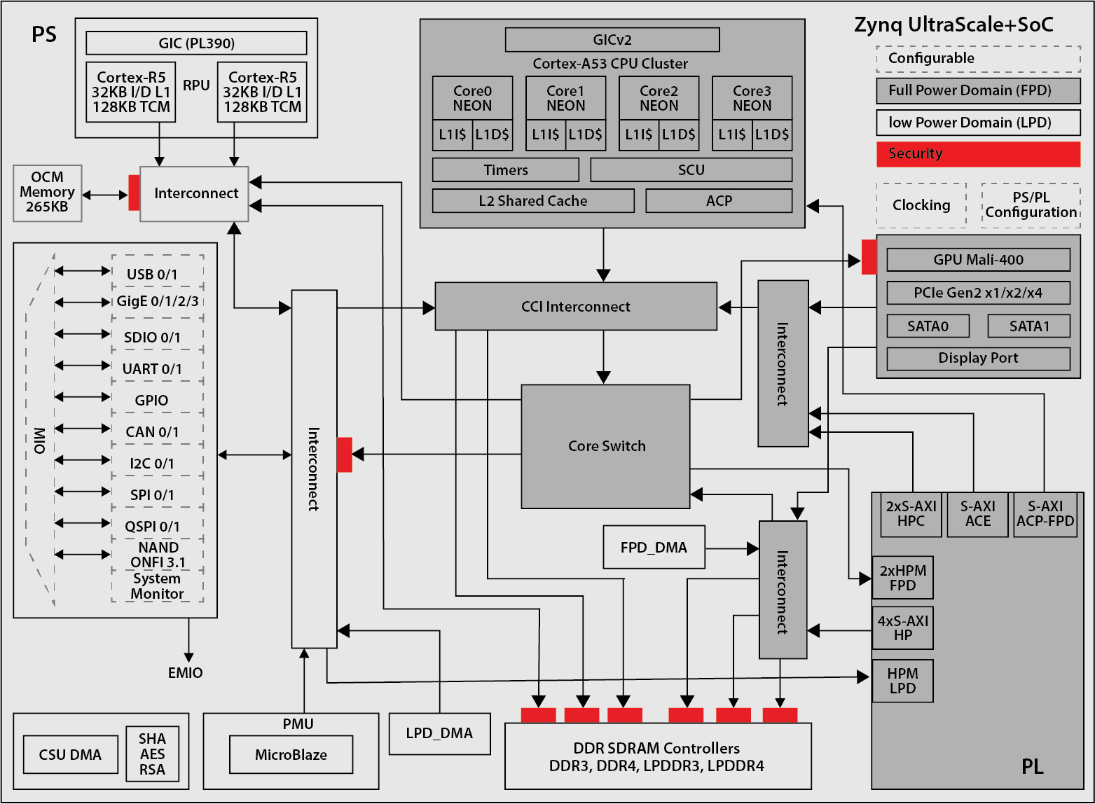
Figure 1.10 – Zynq UltraScale+ MPSoC architecture – quad-core cluster
The following section provides a brief description of the main features of the Zynq UltraScale+ MPSoC. For a detailed technical description, please read the Zynq UltraScale+ MPSoC TRM at https://www.xilinx.com/support/documentation/user_guides/ug1085-zynq-ultrascale-trm.pdf.
Zynq UltraScale+ MPSoC APU
The CPU cluster topology is built around an ARM Cortex-A53 CPU, which comes in a quad-core or a dual-core MPCore. The CPU cores implement the Armv8-A architecture with support for the A64 instruction set in AArh64 or the A32/T32 instruction set in AArch32. Each CPU core comes with an L1 instruction cache with parity protection and an L1 data cache with ECC protection. The L1 instruction cache is 2-way set-associative, while the L1 data cache is 4-way set-associative. It also has its own MMU, an FPU, and a Neon SIMD engine. The CPU cluster has a 16-way set-associative L2 common cache and an SCU with an ACP port that extends cache coherency beyond the cluster with external masters in the PL. Each CPU core provides a performance figure of 2.3 DMIPS/MHz with an operating frequency of up to 1.5 GHz. The CPU core is also TrustZone enabled for secure operations.
The CPU cluster can operate in symmetric SMP and asymmetric AMP modes with the power island gating for each processor core. Its unified Level 2 cache is ECC protected, is 1 MB in size, and is common to all CPU cores and both instructions and data.
The APU has a 128-bit AXI coherent extension (ACE) port that connects to the PS cache coherent interconnect (CCI), which is associated with the system memory management unit (SMMU). The APU has an ACP slave port that allows the PL master to coherently access the APU caches.
The APU has a GICv2 general interrupt controller (GIC). The GIC acts as a distributor of interrupts to the CPU cluster cores according to the user’s configuration, with support for priority, preemption, virtualization, and security. Each CPU core contains four of the ARM generic timers. The cluster has a watchdog timer (WDT), one global timer, and two triple timers/counters (TTCs).
Zynq UltraScale+ MPSoC RPU
The RPU contains a dual-core ARM Cortex-R5F cluster. The CPU cores are 32-bit real-time profile CPUs based on the ARM-v7R architecture. Each CPU core is associated with tightly coupled memory (TCM). TCM is deterministic and good for hosting real-time, latency-sensitive application code and data. The CPU cores have 32 KB L1 instruction and data caches. It has an interrupt controller and interfaces to the PS elements and the PL via two AXI-4 ports connected to the low-power domain switch. Software debugging and tracing is done via the ARM CoreSight Debug subsystem.
Zynq UltraScale+ MPSoC GPU
The PS includes an ARM Mali-400 GPU. The GPU includes a geometry processor (GP) and has an MMU and a Level 2 cache that’s 64 KB in size. The GPU supports OpenGL ES 1.1 and 2.0, as well as OpenVG 1.1 standards.
Zynq UltraScale+ MPSoC VCU
The video codec unit (VCU) supports H.265 and H.264 video encoding and decoding standards. The VCU can concurrently encode/decode up to 4Kx2K at 60 frames per second (FPS).
Zynq UltraScale+ MPSoC PMU
The PMU augments the PS with many functionalities for startup and low power modes, some of which are as follows:
- System boot and initialization
- Manages the wakeup events and low processing power tasks when the APU and RPU are in low-power states
- Controls the power-up and restarts on wakeup
- Sequences the low-level events needed for power-up, power-down, and reset
- Manages the clock gating and power domains
- Handles system errors and their associated reporting
- Performs memory scrubbing for error detection at runtime
Zynq UltraScale+ MPSoC DMA channels
The PS has 8-channel DMA engines that support transactions between memories, peripherals, as well as scatter-gather operations. Their interfaces are based on the AXI protocol. They are split into two categories: the low power domain (LPD) DMA and full power domain (FPD) DMA. The LPD DMA is I/O coherent with the CCI, whereas the FPD DMA is not.
Zynq UltraScale+ MPSoC memory interfaces
In this section, we will look at the various Zynq UltraScale+ MPSoC memory interfaces.
DDR memory controller
The PS has a multiport DDR SDRAM memory controller. Its internal interface consists of six AXI data ports and an AXI control interface. There is a port dedicated to the RPU, while two ports are connected to the CCI; the remaining ports are shared between the DisplayPort controller, the FPD DMA, and the PL. Different types of SDRAM DDR memories are supported, namely DDR3, DDR3L, LPDDR3, DDR4, and LPDDR4.
Static memory interfaces
The external SMC supports managed NAND flash (eMMC 4.51) and NAND flash (24-bit ECC). Serial NOR flash is also supported via 1-bit, 2-bit, Quad-SPI, and dual Quad-SPI (8-bit).
OCM memory
The PS also has an on-chip RAM that’s 256 KB in size, which provides low latency storage for the CPU cores. The OCM controller provides eight exclusive access monitors to help implement inter-cluster atomic primitives for access to shared memory regions within the MPSoC.
The OCM memory is implemented as a 32-bit wide memory for achieving a high read/write throughput and uses read-modify-write operations for accesses that are smaller in size. It also has a protection unit and divides the OCM address space into 64 regions, where each region can have separate security and access attributes.
QSPI flash controller
There are two Quad-SPI controllers in the IOP block of the PS, as follows:
- A legacy Quad-SPI (LQSPI) controller that presents the flash device as a linear memory space on the AXI interface of the controller. It supports eXecute-in-Place (XIP) for booting and running application software.
- A generic Quad-SPI (GQSPI) controller that provides I/O, DMA, and SPI mode interfacing. Boot and XIP are not supported by the GQSPI.
The PS can only use a single controller at a time. The Quad-SPI controllers access multi-bit flash memory devices for high throughput and low pin-count applications.
Zynq-UltraScale+ MPSoC IOs
The PS integrates 4-Gb transceivers that can operate at a data rate of up to 6.0 Gb/s. These transceivers can be used as part of the physical layer of the peripherals for high-speed communication.
PCIe interface
The PS includes a PCIe Gen2 with either x1, x2, or x4 width. It can operate as a root complex or endpoint. It can act as a master on its AXI interface using its DMA engine.
SATA interface
The PS integrates two SATA host port interfaces that conform to the SATA 3.1 specification and the Advanced Host Controller Interface (AHCI) version 1.3. Operation speeds at 1.5 Gb/s, 3.0 Gb/s, and 6.0 Gb/s data rates are supported.
Zynq UltraScale+ MPSoC IOP block
The IOP block contains external communication interfaces. The IOP block includes many external interfaces, such as Ethernet MACs, USB controllers, CAN Bus controllers, SDIO interfaces, SPI and I2C ports, and high-speed UARTs.
Zynq-UltraScale+ MPSoC interconnect
The PS interconnect is formed of multiple switches to connect system resources and is based on the ARM AMBA 4.0. The switches are grouped with high-speed bridges, allowing data and commands to flow freely between them. The PS interconnect has separate segments: a full-power domain (FPD) and a low-power domain (LPD). It has QoS and performance monitoring features. It also performs transaction monitoring to avoid interconnect hangs. The interconnect uses the AXI Isolation Block (AIB) module to isolate ports and allows you to power them down to save power. The interconnect has a CCI-400 to extend cache coherency outside of the APU cluster and an SMMU so that virtual addresses outside of the APU cluster can be used.