Frank Bruno is an experienced high-performance design engineer specializing in FPGAs with some ASIC experience. He has experience working for companies like SpaceX, GM Cruise, Belvedere Trading, Allston Trading, and Number Nine. He is currently working as an FPGA engineer for Belvedere Trading. Read more about Frank Bruno
Guy Eschemann
Guy Eschemann
Guy Eschemann was an Electrical Engineer with over twenty years of experience designing FPGA-based embedded systems for automotive, industrial, medical, aerospace, military, and telecom applications. He was working as an FPGA engineer at plc2 Design GmbH. Read more about Guy Eschemann
Whether you want to accelerate mathematically complex operations such as machine learning or artificial intelligence, or simply want to do some projects for fun, such as retro computing or reproducing obsolete video game machines (https://github.com/MiSTer-devel/Main_MiSTer/wiki), this book will jumpstart your journey. There couldn’t be a better time to get into this field than the present, even if only as a hobby. Development boards are cheap and plentiful, and vendors have started making their tools available for free because of their low-cost, smaller parts.
In this book, we are going to build some example designs to introduce you to FPGA development, culminating in a CPU-based project that can drive a Video Graphics Array (VGA) monitor. Along the way, we’ll interface with Double Data Rate (DDR) memory, temperature sensors, microphones, speakers, and serial ports, often referred to as Universal Asynchronous Receivers/Transmitters (UARTs).
In the this chapter, we will be exploring Field Programmable Gate Arrays (FPGAs) and the underlying technology that creates them. This underlying technology allows companies such as AMD (formerly Xilinx) to produce a reprogrammable chip from an Application-Specific Integrated Circuit (ASIC) process. By the end of this chapter, you should have a good understanding of an FPGA and its components, having covered the following topics:
What is an ASIC?
Introducing FPGAs
Evaluation boards
Technical requirements
This chapter is an optional overview chapter and doesn’t have any technical requirements. We will look at the underlying FPGA and ASIC technology and primitive logic gates in this chapter. If you are already comfortable with this information, please feel free to use this as a reference and jump ahead to Chapter 2, FPGA Programming Languages and Tools.
What is an ASIC?
ASICs are the fundamental building blocks of modern electronics – your laptop or PC, TV, cell phone, digital watch, almost everything you use on a day-to-day basis. It is also the fundamental building block upon which the FPGA we will be looking at is built. In short, an ASIC is a custom-built chip designed using the same language and methods we will be introducing in this book.
Note: This section is for reference and an introduction to basic digital electronics. ASICs and FPGAs are both developed using similar Hardware Descriptive Language (HDL) coding methods. This opens up additional career opportunities for someone with this knowledge.
FPGAs came about as the technology to create ASICs followed Moore’s law (Gordon E. Moore, Cramming More Components Onto Integrated Circuits, Electronics, Volume 38, Number 8, https://archive.computerhistory.org/resources/access/text/2017/03/102770822-05-01-acc.pdf) – the idea that the number of transistors on a chip doubles every 2 years. This has both allowed for very cheap electronics, in the case of mass-produced items containing ASICs, and led to the proliferation of lower-cost FPGAs.
The first commercial FPGA was introduced by Xilinx in 1985, the XC2064. This part is only slightly larger than the Combination Logic Block (CLB)s we’ll look at later, but at the time, it was revolutionary. Prior to this, the only programmable logic was based on Erasable Programmable Memory (EPROM) arrays to implement small logic functions, sometimes with storage elements included on the chip. This was long before HDL languages were used to program the devices and they were often configured with a much simpler syntaxed language.
FPGAs are an ASIC at heart. Xilinx has used an ASIC process to create a reconfigurable chip. However, we must consider the trade-offs in choosing an FPGA or ASIC.
Why an ASIC or FPGA?
ASICs can be an inexpensive part when manufactured in high volumes. You can buy a disposable calculator, a flash drive for pennies/cents per gigabyte, or an inexpensive cell phone; they are all powered by at least one ASIC. ASICs are also sometimes a necessity when speed is of the utmost importance, or the amount of logic that is needed is very large. However, in these cases, they are typically only used when cost is not a factor.
We can break down the costs of developing a product based on an ASIC or FPGA into Non-Recurring Engineering (NRE), the one-time cost to develop a chip, and the piece price for every chip, excluding NRE. Ed Sperling stated the following in CEO Outlook: It Gets Much Harder From Here, Semiconductor Engineering, June 3, 2019, https://semiengineering.com/ceo-outlook-the-easy-stuff-is-over/: “The NRE for a 7nm chip is $25 million to $30 million, including mask set and labor.”
These costs are a necessity to build a chip and the main reason why ASICs, especially very advanced ones, are very expensive to produce. They include more than just the mask sets, the blueprint for the ASIC, if you will, that is used to deposit the materials on the silicon wafers that build the chip. These costs also include the salaries for teams of design, implementation, and verification engineers that can number into the hundreds. Re-spins, or bug fixes, are usually factored into ASIC costs because large, complex devices struggle with first-time success.
Compare this to an FPGA, where complex chips can be developed by a single person or small teams. Most of the NRE has been shouldered by the FPGA vendor in the design of the FPGA chips, which are known good quantities. The little NRE expense left is for tools and engineering. Re-spins are free, except for time, since the chip can be reprogrammed using flash memory, without million-dollar mask sets.
The trade-off is the per-part cost. High-volume ASICs with low complexity, like the one inside a pocket calculator or a digital watch, can cost pennies. CPUs can run into the hundreds or thousands of dollars. Compare that to FPGAs where even the most inexpensive Spartan-7 starts at a few dollars, and the largest and fastest can stretch into tens of thousands of dollars.
Another factor is tool costs. As we will see in Chapter 2, FPGA Programming Languages and Tools, AMD provides the Xilinx Vivado tool suite for free for the smaller parts. Other FPGA vendors, such as Intel (formerly Altera), also offer free versions for lower-end parts. This speeds up adoption, where the barrier to entry is now a computer and a development board. Even the cost of developing more expensive parts is only a few thousand dollars if you need to purchase a professional copy of Vivado for AMD or Quartus for Intel. In contrast, ASIC tools can run into millions of dollars and require years of training since the risk of failure is extremely high. As we will see in our projects, we’ll make mistakes, sometimes to demonstrate a concept, but the cost to fix it will only be a few minutes, mostly spent on understanding why it actually failed.
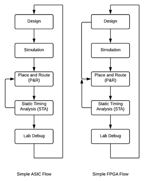
Figure 1.1: Simple ASIC versus FPGA flow
The flow for an ASIC or FPGA is essentially the same as shown above in Figure 1.1. ASIC flows tend to be more linear in that you have one chance to make a working part. With an FPGA, things such as simulation can become an option, although strongly suggested for complex designs. One difference is that the lab debug stage can also act as a form of simulation by using ChipScope, or similar on-chip debugging techniques, to monitor internal signals for debugging. The main difference is that each iteration through the steps costs only time in an FPGA flow. In this situation, any changes to a fabricated ASIC design would require some number of new mask sets, the costs of which could run into the millions of dollars.
We summarize the choice between an ASIC and FPGA in Table 1.1 below:
FPGA
ASIC
Mostly reprogrammable
Limited or no programmability
Very high piece price
Extremely low to high piece price, usually based on volumes
Very low NRE
Very high NRE
Low tool cost
Very high tool cost
Easy to debug in lab/high visibility into design
Usually limited ability to view internal states
Table 1.1: FPGA versus ASIC summary
We’ve briefly looked at what an ASIC is and why we might choose an ASIC or an FPGA for a given application. Now, let’s look at how an FPGA is created using an ASIC process.
How does a company create a programmable device using an ASIC process?
The basis of any ASIC technology is the transistor, with the largest devices made up of billions of transistors. Multiple ASIC processes have been developed over the years, and they all rely on transistors, which can be on or off, represented as 1s and 0s. These can be thought of as Booleans, true or false values.
The basis of Boolean algebra was developed by George Bool in 1847. The fundamentals of Boolean algebra make up the basis of the logic gates upon which all digital logic is formed. The code that we will be writing is at a high level of abstraction from the actual hardware implementation and the tools will convert our design into a physical implementation. It is important to understand the basics and will give us a good springboard for a first project. Thousands of engineers have struggled to build efficient logic by hand in the past using individual ICs on a breadboard. I want to get you past that with a minimum of fuss since modern tools are very good at what they do.
An FPGA company, such as AMD or Intel, develops an FPGA by creating configurable structures that can be loaded at the initialization of the device or modified during runtime. The same techniques we will talk about here are used to design blocks that are then synthesized directly into transistors rather than mapped to lookup tables and routing resources. The interesting thing about the fact that the same design techniques are used for FPGAs and ASICs is that many ASICs are prototyped on FPGAs to minimize logic errors and re-spins.
We’ll need to know a little Hardware Description Language (HDL) such as Very High Speed Integrated Circuit HDL (VHDL) or SystemVerilog to go through this section.
Introduction to HDLs
We’ll need to define some terminology for discussing HDLs.
Logical versus bitwise operations
Logical functions operate on Boolean values. A Boolean is an object that can hold one of two values: true or false for VHDL, and 1 or 0 for SystemVerilog/Verilog. SystemVerilog/Verilog has no concept of true and false. Note that this can be viewed as an advantage of SystemVerilog as it behaves like hardware in that there is no difference between a 1 and true or 0 and false when you implement hardware. VHDL proponents view the strong typing of VHDL as an important feature since it clarifies intent by forcing the correct types to be used.
A bitwise function operates on a 1 or 0 (or as we will discuss later in the book, other values representing unknown, tri-state or different drive strengths). Both VHDL and SystemVerilog/Verilog have objects that hold these values and are operated on in a bitwise function. We will dive deeper into this in Chapter 3, Combinational Logic, but we’ll be using if statements in some of the examples below to demonstrate the logic gates.
Bitwise functions also have the ability to act as reduction operators in SystemVerilog/Verilog and there are similar functions in VHDL. These will be discussed in Chapter 2, FPGA Programming Languages and Tools.
In this section, we are primarily discussing logical functions. In SystemVerilog and Verilog, logical and bitwise functions can be intermixed as they are weakly typed languages. VHDL is strongly typed and you will run into problems mixing them up. This will be discussed further in Chapter 3.
Armed with this knowledge, let’s dip our toes into some HDL code.
Creating gates using HDL
In this section, we’ll take a look at some basic HDL code that will allow us to demonstrate the gates that underlie all digital designs. We need a way of inferring these operations and we’ll start by looking at signal assignments.
Assign statement (SystemVerilog/Verilog)
We can use an assign statement to take whatever value is on the right-hand side (RHS) of the equal sign to the left-hand side (LHS). Its usage is as follows:
assign out = in;
in can be another signal, function, or operation on multiple signals. out can be any valid signal declared prior to the assign statement. The above code simply acts like a wire.
Assign statement equivalent (VHDL)
In VHDL, a signal can be assigned as follows:
output <= input;
Similar to SystemVerilog/Verilog, whatever is on the RHS will be assigned to the LHS.
in and out are reserved words used for port directions in VHDL. input and output are reserved words used for port direction in SystemVerilog, hence the signal name changes between language examples.
Single line comments
SystemVerilog and VHDL both provide a method for creating a comment on a single line. The comment runs from the comment character, which is // for SystemVerilog or – for VHDL, until the end of the line:
// Everything here is a comment. (SystemVerilog)-- Everything here is a comment. (VHDL)
Multiline comments
Both SystemVerilog and Verilog share the same type of multiline comments, based upon the C style of comment. Block comments have also been supported in VHDL since 2008:
/*
   I can span    Multiple    Lines
 */
Prior to VHDL-2008, VHDL only supported single line comments (–).
if statement
Both SystemVerilog/Verilog and VHDL provide a way of testing conditions via the if statement. The basic syntax is as follows:
if (condition) …; // SystemVerilog/ Verilogif condition then ... endif; // VHDL
The if statement will be used throughout the book and there are some nuances that we will discuss in more detail in Chapter 3, Combinational Logic.
With the terminology out of the way, let’s look at Boolean logic gates used Boolean operations.
Fundamental logic gates
There are four basic logic gates. These gates are necessary for anything from simple control logic to complex arithemetic and processing algorithms. AI is all the rage at the time of authoring this book and the heart of every AI system boils down to these simple structures.
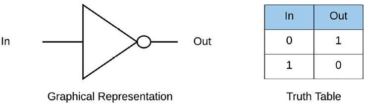
We typically write the truth tables for the gates to understand their functionality. A truth table shows us what the output is for every set of inputs to a circuit. Refer to the following example involving a NOT gate.
Logical NOT
The output of the NOT gate produces the opposite value of a signal going in. It’s often called an inverter since it inverts the value. The function in SystemVerilog can be written as follows:
assign out = !in; // logical NOT Boolean operator
In VHDL, we would write:
out <= notin; // Boolean operator
The associated truth table is as follows:
Figure 1.2: NOT gate representation
The NOT gate is one of the most common operators we will be using:
if (!empty) ... // SystemVerilog/Verilogifnot empty then .– -- VHDL
Often, we need to test a signal before performing an operation. For example, if we are using a First In, First Out (FIFO) storage to smooth out sporadic data or for crossing clock domains, we’ll need to test whether there is data available before popping it out for use. FIFOs have flags used for flow control, the two most common being full and empty. We can do this by testing the empty flag, as shown here.
We will go into greater depth in later chapters on how to design a FIFO as well as use one.
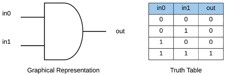
Logical AND
Often, we will want to test whether one or more conditions are active at the same time. To do this, we will be using the AND gate. An AND gate tests two or more inputs to determine if all of them are set. If any input is a 0, the AND gate will return a 0. If all of them are set, it will return a 1.
The function in SystemVerilog/Verilog can be written as follows:
assign out = in1 && in0; // logical AND Boolean operator
The function in VHDL can be written as follows:
out <= in1 and in0; -- logical AND Boolean operator
The associated truth table is as follows:
Figure 1.3: AND gate representation
Continuing our FIFO example, you might be popping from one FIFO and pushing into another:
if (!src_fifo_empty && !dst_fifo_full) ... // SV/ Verilogif (not src_fifo_empty) and (not dst_fifo_full) then .– -- VHDL
In this case, you want to make sure that both the source FIFO has data (i.e., is not empty) and that the destination is not full. We can accomplish this by testing it via the if statement.
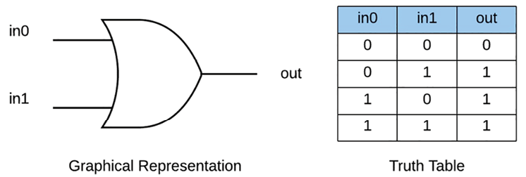
Logical OR
Another common occurrence is to check whether any one signal out of a group is set to perform an operation. An OR gate tests two or more inputs to determine if any of them are set to a 1. If any input is a 1, then the output will be a 1. If all inputs are 0, then the output is a 0.
The function in SystemVerilog/Verilog can be written as follows:
assign out = in1 || in0; // logical Boolean operator
The function in VHDL can be written as follows:
out <= in1 or in0; // logical Boolean operator
The associated truth table is as follows:
Figure 1.4: OR gate representation
Next, we will look at the exclusive OR function.
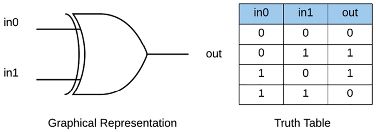
XOR
The exclusive OR (XOR) function checks whether either one of two inputs is set, but not both. XOR functions test whether an odd number of inputs are set to a 1 if you have more than two inputs.
The function in SystemVerilog/Verilog can be written as follows:
assign out = in1 ^ in0; // XOR Boolean operator
The function in VHDL can be written as follows:
out <= in1 xor in0; -- XOR Boolean operator
The associated truth table is as follows:
Figure 1.5: XOR gate representation
This function is used in building adders, parity, and error-checking and correcting code. In the next section, we’ll look at how an adder is built using the preceding gates.
More complex operations
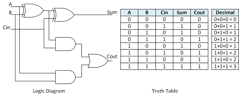
We’ve seen the basic building blocks in the previous sections that make up every digital design. Here, we’ll look at an example of how we can put together multiple logic gates to perform work. For this, we will introduce the concept of a full adder. A full adder takes three inputs, A, B, and carry in (Cin), and produces two outputs, Sum and Carry out (Cout). Let’s look at the truth table of a full adder.
Figure 1.6: Full adder
Algebraically, a full adder represents A + B + Cin. Each input is a single bit, so the output could be 0, 1, or 2 in decimal. Since we can only represent 0 and 1 in a single bit, if the addition produces a result of 2, that represents a carry out. The carry out would propagate into the next bit. This cascading of full adders is called a ripple carry adder, since they carry ripples from one cell to the next.
The SystemVerilog/ Verilog for the full adder written as Boolean logic would be as follows:
assign Sum = A ^ B ^ Cin;
assign Cout = A & B | (A ^ B) & Cin;
You’ll notice that we are using the bitwise operators for AND (&) and OR (|) since we are operating on bits. These are equivalent to the logical operators AND (&&) and OR (||). This is true for SystemVerilog/Verilog, but not in VHDL.
The VHDL code for the full adder written as Boolean logic would be as follows:
Sum <= A xor B xor Cin;
Cout <= (A and B) or ((A xor B) and Cin);
From this straightforward yet important example, you can see how real-world functionality can be built from these basic building blocks. All the circuits in an ASIC or FPGA are built this way, but luckily, you don’t need to dive into this level of detail unless you want to thanks to the proliferation of HDLs such as SystemVerilog/Verilog and VHDL.
With this basic understanding of gates and logic under our belts, we can look at FPGAs.
Introducing FPGAs
A gate array in ASIC terms is a sea of gates with some number of mask steps that can be configured for a given application. This allows for a more inexpensive product since the company designing the ASIC only needs to pay for the masks necessary for configuring. The FPGA takes this one step further by providing the programmability of the fabric as part of the device. This results in an increased cost as you are paying for the interconnect you are not using and the storage devices necessary to configure the FPGA fabric but allows for cost reductions as these parts become standard devices that can be mass produced.
If we look at the functions in the previous section through the adder example, we can see one commonality; they can all be produced using a truth table. This becomes key in FPGA development. We can regard these truth tables as Read-Only Memory (ROM) representations of the functions. In fact, we can regard them as Programmable ROMs (PROMs) in the case of building up our FPGA.
If you look at the truth table for the full adder, you can see that there are three inputs and two outputs. If we look at the inputs as an address, then we could use storage to look up the data stored at that location and use it as an output. A ROM can be very tiny since it is hardcoded to look up certain values. A PROM uses some storage elements that can be changed to implement new functions, which is closer to what we will use in the FPGA.
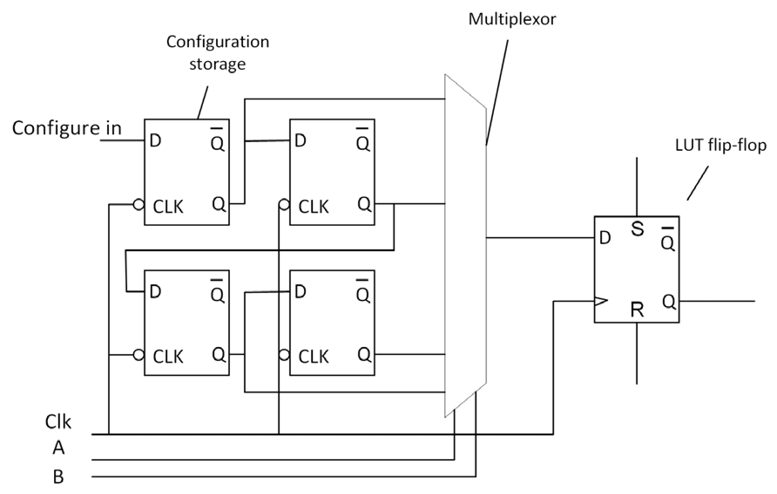
Let’s take the example of the fundamental logic functions. We can reproduce any of them by utilizing a two-input lookup table, which could look something like this:
Figure 1.7: Two-input LUT examples
In Figure 1.7, we can see an oversimplified example with four storage elements, in this case, flip-flops (configuration storage), but in the case of an actual FPGA, we would more likely have a much simpler structure utilizing far fewer transistors. We will discuss storage elements in Chapter 4, Counting Button Presses. The storage elements are connected to one another such that their configuration can be loaded. By attaching other Lookup Tables (LUTs) to the chain, multiple LUTs can be configured at startup or, in the case of partial reconfiguration, during normal operation.
We have a component called a MUX, or multiplexor, that acts as the address lookup by selecting the storage element pointed to by the address made up of inputs A and B. This gives us the value at that location. If you look back at our two input gates, you should be able to see that we can map any two-input gate to this structure. By adding a flip-flop, we can see the final structure of the LUT takes shape.
The power of the simplicity of the structure is the ability to replicate this design many times over. In the case of modern FPGAs, they are built of many tiles or columns of logic such as this, allowing a much simpler piece to be designed, implemented, verified, and then replicated to produce the large gate count devices available. This allows for a range of lower-cost devices with fewer columns of resources to larger devices with many more, some even using Stacked Silicon Interconnects (SSIs), which allows multiple ASIC dies to be attached via an interconnect substrate.
In 1985, Xilinx introduced the XC2064, which was what we would consider the first FPGA utilizing an array of 64 three-input LUTs with one flip-flop. The breakthrough with this design was that it was modular and had good interconnect resources. This entire part would be approximately equivalent to one CLB in the Artix-7 we will be targeting.
The combinational logic blocks would be useless if we didn’t have a way for them to communicate with each other. This is where programmable interconnect gets involved. The FPGA fabric consists of LUTs with associated flip-flops making up slices and, ultimately, CLBs. These blocks are all connected using a rich topology of routing channels, allowing for almost limitless configuration. FPGAs also contain many other resources that we will explore over the course of this book, block RAMs, Serial-Deserial (SERDES) cores, Digital Signal Processing (DSP) elements, and many types of programmable Input/Output (I/O).
We’ve seen the theory of a simple device, but this isn’t really that useful today. Next, we will look at the FPGAs, which, although a few years old, are still great devices to choose for hobbyists and low-cost designs.
Exploring the Xilinx Artix-7 and 7 series devices
The FPGA we will be looking at in this book is an Artix-7 device. These devices have the highest performance per watt of the Xilinx 7 series devices. For a reasonable price, they feature a large amount of relatively high-performance logic to implement your designs. The FPGA components we will introduce here are common in the Artix (low-end), Kintex (mid-range), and Virtex (high-end) parts in the 7 series.
Combinational logic blocks
ASICs are made up of logic gates based upon libraries provided by ASIC foundries, such as Taiwan Semiconductor Manufacturing Company and Tower Semiconductor. These libraries can contain everything from AND, OR, and NOT gates to more complicated math cells and storage elements. When developing an FPGA, you will be targeting the same Boolean logic equations as you would in an ASIC. We will be using a very similar flow. However, the synthesis process will target the CLBs of the FPGA:
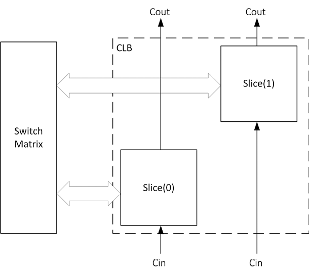
Figure 1.8: CLB internals
A CLB consists of a pair of slices, each of which contains four six-input LUTs and their eight flip-flops. Vivado (or optionally a third-party synthesis tool such as Synopsys Synplify) compiles the SystemVerilog/Verilog or VHDL code and maps it to these CLB elements. To fully explore the details of the CLB, I would suggest reading the Xilinx UG474, 7 Series FPGAs CLB user guide (https://www.xilinx.com/support/documentation/user_guides/ug474_7Series_CLB.pdf). At a high level, each LUT allows a degree of flexibility such that any Boolean function with six inputs can be implemented or two arbitrarily defined five-input functions if they share common inputs. There is also dedicated high speed carry logic for arithmetic functions, which will be discussed in later chapters.
The slices come in two formats, SLICEL (L = logic), which can only implement logic functions and storage elements, and SLICEM (M = memory), which additionally can be reconfigured for use as a small memory element (distributed RAM) or a shift register. There are approximately three times the number of SLICELs as SLICEMs. The following table, for the one suggested development board for this book, shows the breakdown:
Board
Device
Slices
SLICEL
SLICEM
6-Input LUTs
Distributed RAM (Kb)
Shift Register (Kb)
Flip-Flops
Nexys A7
7A100T
15,850
11,100
4,750
63,400
1,188
594
126,800
Table 1.2: Nexys A7 FPGA resources
Although it is possible to instantiate and force the functionality of lower-level components, such as slices or LUTs, this is beyond the scope of this book, and a feature not widely used. We will be targeting CLB usage through the synthesis of the HDL that we write.
Storage
Aside from the SLICEMs that make up the CLBs that can be used as memories or shift registers, FPGAs contain Block RAMs (BRAMs) that are larger storage elements. The 7 series parts all have a 36 Kb BRAM that can be split into two 18 Kb BRAMs. The recommended development board, the Nexys A7 with the 100T part has 135 BRAMs, 36Kb each.
In normal computer parlance, Kb is kilobits, while KB is kilobytes – lowercase b for bits, and uppercase B for bytes.
BRAMs can be configured as follows:
True dual port memories – Two read/write ports.
Simple dual port memories – 1 read/1 write. In this case, a 36-Kb BRAM can be up to 72 bits wide and an 18-Kb BRAM up to 36 bits wide.
A single port.
The contents of BRAMs can be loaded at initialization and configured via a file or initial block in the code. This can be useful for implementing ROMs or start-up conditions.
BRAMs in 7 series devices also contain logic to implement FIFOs. This saves CLB resources and reduces synthesis overhead and potential timing problems in a design. We will go over FIFOs in a later chapter.
All 36-Kb BRAMs have dedicated Error Correction Code (ECC) functions. As this is something more related to high-reliability applications, such as medical-, automotive-, or space-based, we will not go into detail on it in this book.
Clocking
7 series devices implement a rich clocking methodology, which can be explored in detail in the UG472 7 series FPGAs clocking resources user guide (https://www.xilinx.com/support/documentation/user_guides/ug472_7Series_Clocking.pdf). For most purposes, our discussion in the Phase Locked Loop (PLL) section will give you everything you need to know; however, the referenced document will delve into far more detail.
I/Os
For the most part, we will limit ourselves to the I/Os supported by the two targeted development boards. In general, the 7 series devices handle a variety of interfaces from 3.3v CMOS/TTL to LVDS and memory interface types. The boards we are using will dictate the I/Os defined in our project files. For more information on all the supported types, you can reference the UG471 7 Series FPGAs SelectIO resources user guide.
DSP48E1 – Xilinx DSP core in 7 series devices
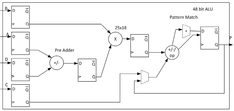
FPGAs have a large footprint in DSP applications that use a lot of multipliers and, more specifically, Multiply Accumulate (MAC) functions. One of the first innovations in FPGAs was to include hard multipliers, which were quickly replaced by DSP blocks that could implement MAC functions. Figure 1.9 shows the implementation of the DSP48E1 implemented in the Artix-7.
Figure 1.9: Xilinx UG479 7 series DSP48E1
One of the most expensive operations in an FPGA is arithmetic. In an ASIC, the largest and slowest operation is typically a multiplication operation, and the smaller or faster operation is an add operation. For this reason, for many years, FPGA manufacturers have been implementing hard arithmetic cores in their fabric. This makes the opposite true in an FPGA, where the slower operation is typically an adder, especially as the widths get larger. The reason for this is that the multiply has been hardened into a complex, pipelined operation. We will explore the DSP operator more in later chapters. The UG479 7 Series DSP48E1 user guide (https://www.xilinx.com/support/documentation/user_guides/ug479_7Series_DSP48E1.pdf) is a good reference if you are interested in delving into the details.
ASMBL architecture
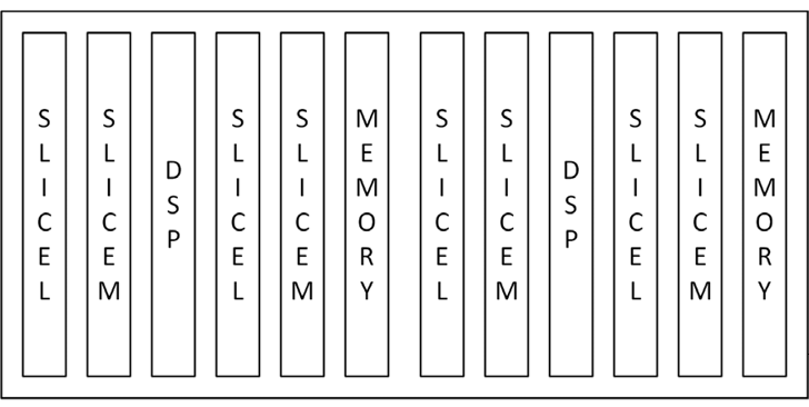
The 7 series devices are the fourth generation where Xilinx has used the Advanced Silicon Modular Block (ASMBL) architecture for implementation purposes. The idea behind this is to enable FPGA platforms to be optimized for different target applications. Looking at the 7 series families, we can see how different configurations of slices are brought together to achieve these goals. We can see how the pieces we covered in this chapter are arranged as columns to give us the resources we will be using for our example projects ahead. Figure 1.10 below shows the internal configuration of the FPGA, which is built by implementing vertical columns of different element types. From the point of view of the FGPA vendor, this simplifies the design and testing of new devices by simply adding more columns, or expanding columns vertically to make larger devices.
Figure 1.10: Example FPGA internal layout based upon ASMBL
Now that we have looked at what makes up the Artix-7 and other 7 series devices, we need to get the Xilinx tools installed so that we can get to our first project.
We’ve looked at FPGAs and the specific FPGA we will target in the book. Now let’s look at the evaluation board that we will target in the book.
Evaluation boards
There is no shortage of FPGA evaluation boards available for us to purchase. One company that makes very affordable boards is Digilent. There are several nice features that its boards tend to include, but one of the best is that they have a built-in USB-to-UART controller that Xilinx Vivado recognizes as a programming cable. This makes configuring the device painless. The recommended boards also have the added advantage of being powered over this same USB cable.
The Nexys A7 is the recommended board for this book. It has all the devices we’ll target over the course of the book.
Nexys A7 100T (or 50T)
Figure 1.11 below is a picture of the Nexys A7 board. There are two variants of the board at the time of writing, the 100T variant and the 50T variant. The difference is only the size of the device installed on the board.
Figure 1.11: Digilent Nexys A7 board
The board features are as follows:
Artix-7 XC7A100T or 50T
450+ MHz operation
128 MB DDR2
Serial flash
Built-in USB UART for downloading images and ChipScope debugging
MicroSD card reader
10/100 Ethernet PHY
PWM audio output/microphone input
Temperature sensor
3-axis accelerometer
16 switches
16 LEDs
5 push buttons
Two 3-color LEDs
Two 4-digit 7-segment displays
USB host device support
Five PMOD (one XADC)
Let’s take a look at the breakdown of the two devices that the Nexys board can be ordered with:
Device
XC7A100T-1CSG324C
XC7A50T-1CSG324C
Logic slices
15,850
8,150
BRAM (Kbits)
4,860
2,700
Clock management tiles
6
5
DSP
240
120
Table 1.3: Breakdown of the devices
One benefit of choosing the XC7A100T is the additional RAM. Especially at the start, you may find yourself relying on chip debugging using ChipScope, and the additional RAM will allow for additional storage for wider busses or longer capture times. We’ll discuss ChipScope in the later chapters.
Summary
In this chapter, we’ve learned the basics of ASICs and FPGAs, how they are built, and when they make monetary sense. We’ve looked at the basic building blocks and gates, and learned how larger components are built from these fundamental cells. We’ve also identified other FPGA components, namely, DSP, BRAM, and PLLs, which we will use throughout the book.
The next chapter will discuss SystemVerilog/Verilog and VHDL, detailing some of the commonalities and differences and why you might pick one over the other. We’ll load up Vivado, develop our first application, and run it.
Questions
When might you use an FPGA?
You are prototyping an application that may eventually be an ASIC.
You will only have very small volumes.
You need something that you can easily change the algorithms on in the future.
All of the above.
When would you use an ASIC?
You are developing a very specialized application, with just a small number to be built and the budget is tight.
You’ve been asked to design a calculator that will be mass produced and that requires a custom processor.
You need something extremely low power and cost is not a consideration.
You are developing an imaging satellite and want the ability to update the algorithms over the lifetime of the satellite.
a, b, and c.
We have seen a full adder in the chapter. A half adder is a circuit that can add two inputs; in other words, no carry in. Can you complete the truth table for the sum and carry for a half adder?
Answers
When might you use an FPGA?
All of the above.
When would you use an ASIC?
a, b, and c.
We have seen a full adder in the chapter. A half adder is a circuit that can add two inputs, in other words, no carry in. Can you complete the truth table for the sum and carry for a half adder?
A
B
Sum
Carry
0
0
0
0
0
1
1
0
1
0
1
0
1
1
1
1
Further reading
Please refer to the following links for more information:
Frank Bruno is an experienced high-performance design engineer specializing in FPGAs with some ASIC experience. He has experience working for companies like SpaceX, GM Cruise, Belvedere Trading, Allston Trading, and Number Nine. He is currently working as an FPGA engineer for Belvedere Trading. Read more about Frank Bruno
Guy Eschemann
Guy Eschemann was an Electrical Engineer with over twenty years of experience designing FPGA-based embedded systems for automotive, industrial, medical, aerospace, military, and telecom applications. He was working as an FPGA engineer at plc2 Design GmbH. Read more about Guy Eschemann